
1st July – Initial ponderings
I need a bidirectional isolated DC/DC converter to work between 24V LiFePO4 batteries and the 380V DC bus required by my grid connected inverter. Join me on my journey trying to build one.
There are a number of different DC/DC converter topologies. Resonant converters have the highest efficiency and produce the least EMI by using zero voltage switching of the MOSFETs. On this page I shall document my progress building a series resonant CLLLC dual active bridge converter. I am starting from scratch. This site is not a guide – it’s more of a journal.
System Specs I’d like to achieve:
- Input voltage: 24-28V (Nominally 26V)
- Output voltage: 370-420V (Nominally 380V)
- Bidirectional Power: 500W
Why this input voltage range?
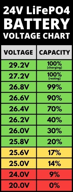
LiFePO4 batteries have extremely flat discharge curves:

A 24V (8 Cell) LiFePO4 battery has a nominal terminal voltage of 26.3V. A search of the web repeatedly shows this SoC-voltage chart:
It therefore makes sense to optimise the system to work between 26V and 380V. This is done by choosing the transformer turns ratio to be 26/380. The resonant controller can slightly adjust its gain to keep the output voltage within the specifications despite a variable input voltage. The inverter can accept a fairly broad voltage range for it’s DC bus.
LiFePO4 batteries last longer if they are operated at lower depths of discharge. It’s common to operate between 10-90% SoC which conveniently reduces the input voltage range to 24-28V.
Learning about resonant converters
Resonant converters can adjust their gain but they work more efficiently when this doesn’t have to happen by much. I found some brilliant resources on resonant converters that’ll better explain their theory than I ever could:
- Infineon Ap note – Resonant LLC Converter: Operation and Design
- TI Design Review – Designing an LLC Resonant Half-Bridge Power Converter
- onsemi – Half-Bridge LLC Resonant Converter Design
- ST Ap note – An introduction to LLC resonant half-bridge converter
Trialing a 12-380V resonant converter:
I read these articles and decided to throw together a quick and dirty unidirectional converter to get a feel for them. I just used parts I had lying around. This setup could convert 12V to 380V:
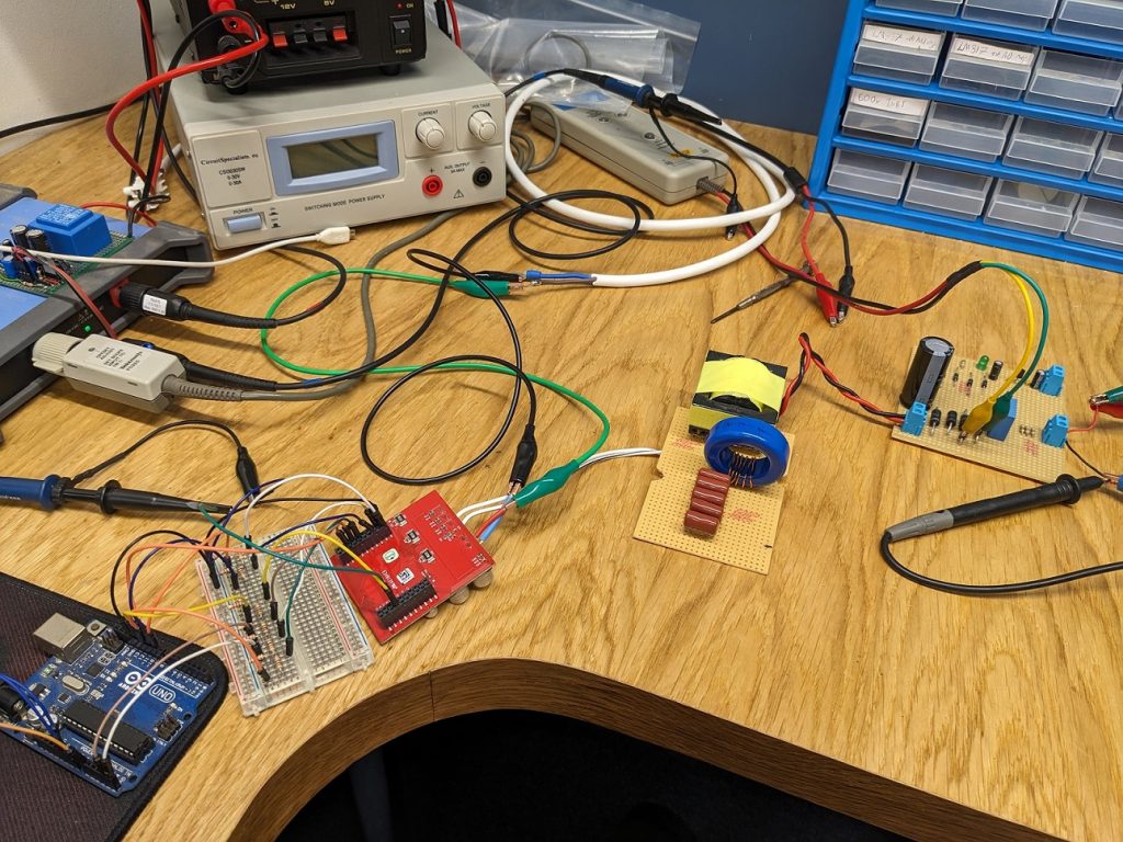
From left to right:
- Arduino Uno (It is connected to a potentiometer) – This produces a frequency adjustable square wave for us between 25-50kHz and SPI interfaces with the BOOSTXL-DRV8301.
- Some level shifting 5-3.3V
- BOOSTXL-DRV8301 – H-Bridge module – Had this lying around.
- The resonant tank
- A simple full bridge rectifier with MUR460 ultrafast 600V diodes
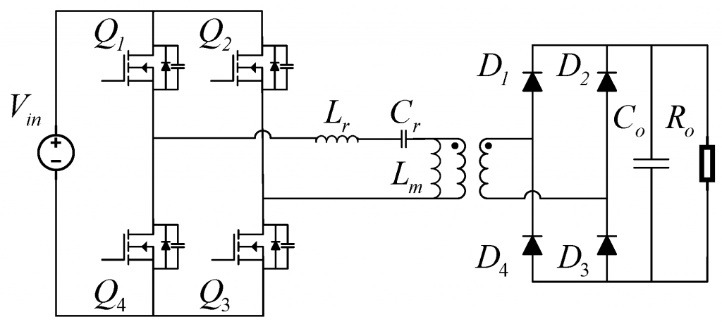
This is the topology used:
The switching transformer was hacked from an inverter board I once got off amazon. I measured the various turns ratios and the magnetising inductance:
I worked through the design steps outlined in the Infineon Ap note:
- I used transformer taps 1-2:4-6 giving a turns ratio of 1:33 and Lm = 42uH
- Decide on Qmax = 0.4
- Choose m = 6.3
- I had rather limited loads that I could dump 400V into. I built up a 5Kohm load from 10K resistors that can just about dissipate 32W without burning up (see below)
- Hence minimum normalised switching Freq = 0.489
- Reflected load resistance = (8/pi^2)*(1/32.6^2)*5000 = 3.81ohms
- Since we want m = 6.3 and Lm = 42uH it follows that Lr = 7.9uH
- I wound 6 turns onto this core and got Lr = 8uH
- It follows our Cr should equal 3.4uF (I managed Cr = 3.7uF)
- It follows that the resonant frequency should be Fr = 29.3kHz
Testing the design:
The converter took a 12.3V input at 2.8A and produced 380V across a 5Kohm load. This equates to a modest efficiency of 83% which I was a little disappointed by.
4th July – Bidirectionality
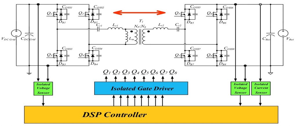
Bidirectional converters need H-Bridges on both sides. That’s why these systems are called dual active bridge converters. To me, it makes sense to have a symmetrical topology to the resonant tank (ie. a CLLLC). I don’t yet understand how the switching control works for these bidirectional circuits. I found these two papers which shines light on the topic:
Design of an Isolated Bidirectional Symmetric Resonant Converter, 2020, Yih-Her Yan et al
CLLLC circuits behave slightly differently from unidirectional systems. In Yih-Her Yan et al it provides gain equations for forward and backward conversions. I entered these equations into a spreadsheet so I could play around with component values and get a feel for gain vs frequency. Here’s the forward gain curve for a 500W and 50W load respectively (Cr1=8uF, Lr1=2uH, Lm=20uH, g1=1, m1=1):
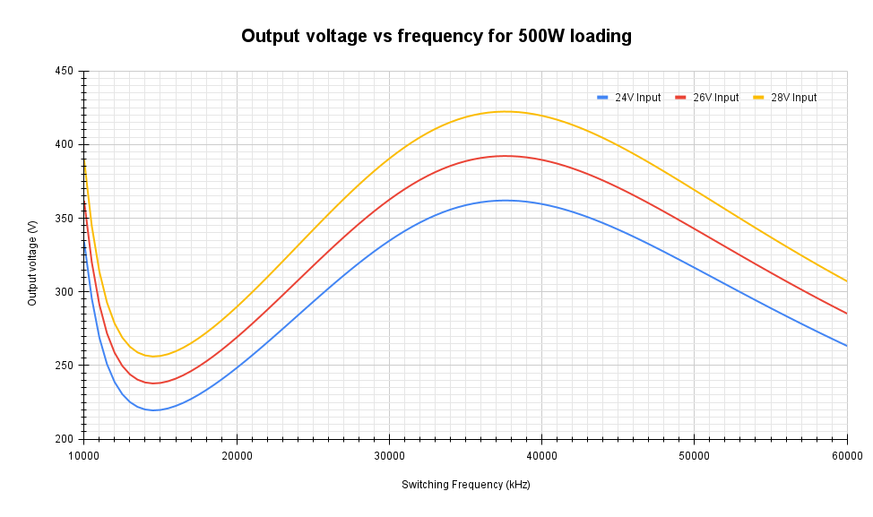
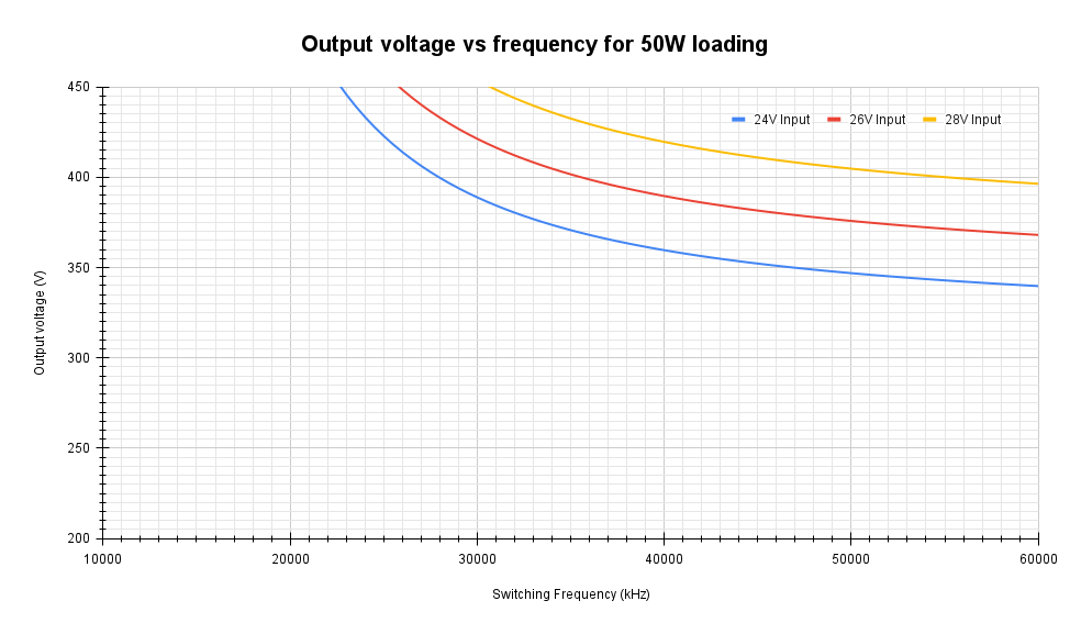
The gain is always 1 at the resonant frequency of 39kHz. With a 24V input the output voltage with 500W load droops below 370V. This wouldn’t be enough for the inverter so it’d have to throttle its output to prevent this. We’ll operate the inverter and CLLLC converter like so:
- The inverter will operate to output as much power as it can without pulling it’s input voltage below 370V or raising it above 420V (depending on power flow direction)
- The CLLLC converter will operate at its resonant frequency unless it has to adjust its gain to keep input/output voltages within range. (eg. with a 24V input it’ll have to reduce it’s switching frequency to increase it’s gain to reach 370V) The CLLLC converter will be designed so that the inverter will be the limiting factor on power flow
For the component choices on the high voltage side I exactly mirrored the values (i.e. set g1 = m1 = 1). Lr2 = Lr1 x N^2 and Cr2 = Cr1 / N^2. This resulted in Lr2 = 450uH and Cr2 = 36nF. As such the gain curves in the forward and backward directions are entirely symmetrical and equal.
What voltage and current sensing do I need and where do I put these sensors? Undoubtedly I need to know the voltages on each side of the converter for the control systems to make appropriate adjustments. Do I need 2 current sensors, 1 for each side of the resonant tank? Or will one 1 suffice? The former paper measures on 1 side. I’d like to avoid complexity wherever possible and currents on either side of the transformer should be proportional to one another (except in a fault condition…). Let’s risk it for now!
There are a number or methods and positions one can place the current sensing. Using a current shunt on the low voltage / high current side would result in big losses (circulating currents ~25A). Sensing on the high voltage / low current side should be much more efficient so is what I went with. I decided on low side current sensing because it avoids the need for a further mini-transformer to generate another isolated supply.
6th July – Learning about switching Transformers
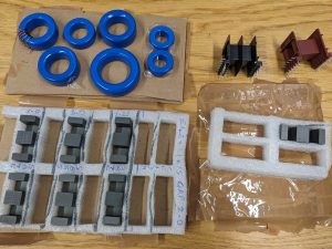
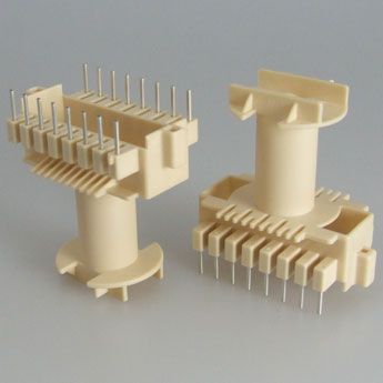
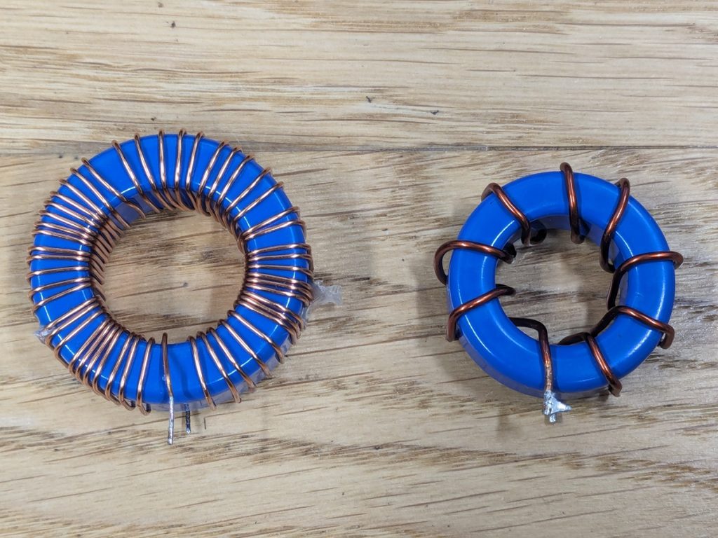
I haven’t started designing the PCB yet… I have been trying to better understand the transformers used in switched mode power supplies (SMPS). In a rush the other day I ordered a load of toroidal cores, ferrite E cores and bobbins to experiment with. Here’s half of the order:
I thought I’d wind my own transformers which has been a great (plus tedious) learning curve. I have made a number of mistakes and wasted most of yesterday achieving very little.
My first transformer (left) had a 4mm air gap. (Here’s a good read on gaps) I was trying to get the magnetizing inductance down so that I could have a higher resonant frequency. I put it into my test circuit and it failed to do anything particular useful. I think for these reasons:
- With the large air gap and the coils separated as they are I think there was flux fringing and a high leakage inductance. I didn’t factor this leakage inductance into the Lr inductance in my test circuit so probably had a very low M-value and therefore high circulating currents.
- I think the magnetising inductance was about 8uH and I don’t think I choose a low enough series resonant inductance Lm.
- The primary coil was getting quite hot. I suppose this was testament to high circulating currents. I think it’s better to have multiple strands than one fat wire due to the skin effect. Also, flux fringing apparently causes eddy currents and further losses.
My second transformer on the right was a complete waste of time! It uses a sendust toroidal core with a permeability u=26. I was trying to go for total flux containment and a distributed air gap. I tediously wound 8 turns for the primary (4 paralleled 0.71mm strands) and 120 turns for the secondary with insulating tape between layers. Took me about 3 hours and again didn’t do anything exciting.
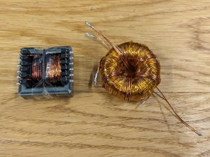
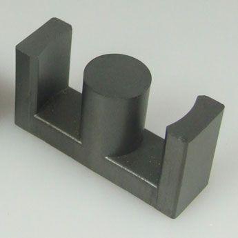
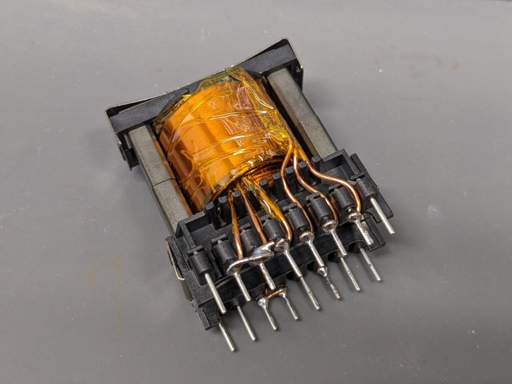
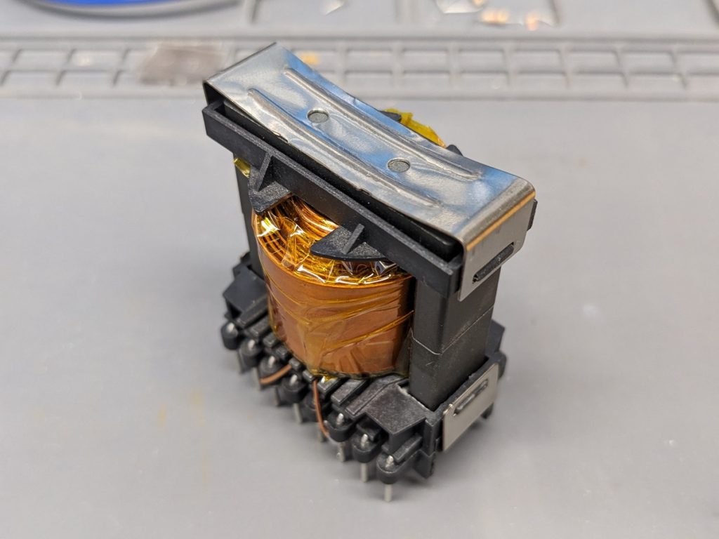
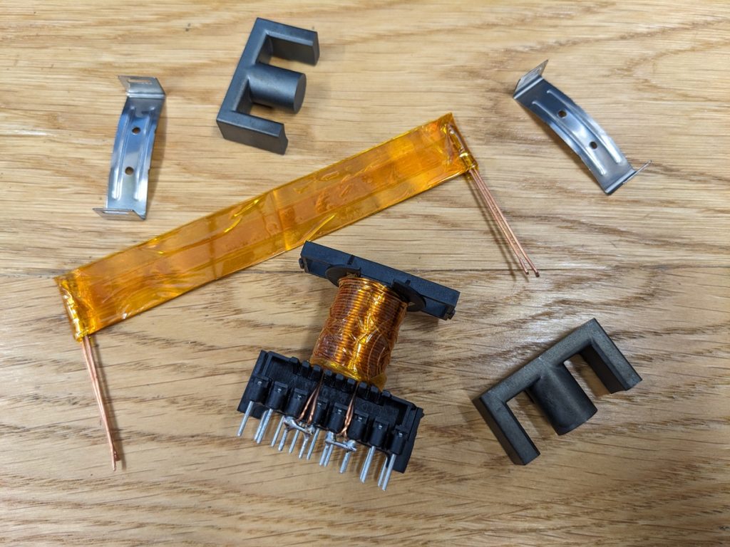
I watched a number of videos to learn how people wounds SMPS coils (Here’s a good winding demo by DiodeGoneWild). I also decided to dissect the hacked SMPS transformer I initially had success with:
There was no air gap and only 3 turns on the primary. These were turns of a flat strip of copper. How very sensible! I had measured the inductance of these 3 turns to be 40uH, which I feel is quite large.
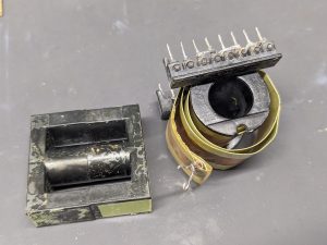
I built my third transformer:
I wound 8 turns on the primary (6 strands of 0.7mm enamelled copper wire) and 121 turns on the secondary. The gap is 1.8mm. I measured the inductance to be 11uH. I put it in my test rig with a Lr=1.94uH inductor and Cr=4uF:
This setup worked beautifully! I powered a 1Kohm load to 380V (140W) with 92% efficiency. The resonant frequency was about 57kHz. I’m confident that I can build an appropriate transformer now. I think I will build the 4th one with these changes:
- Use a vertical EDT core – Nice circular windings and takes up less PCB space
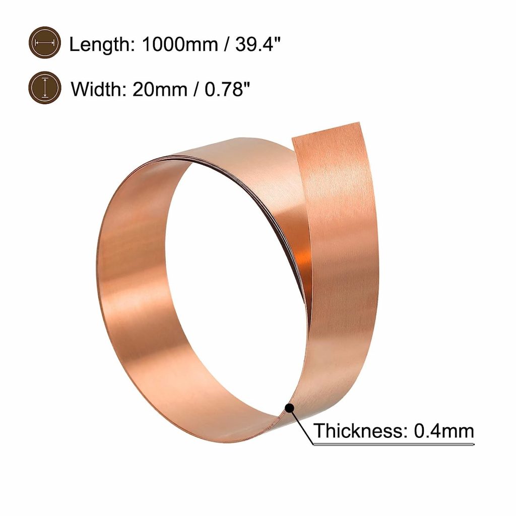
- Use copper strip for the primary – minimal skin effect and excellent copper density
- Aim for 4-5 turns and a tiny gap to achieve a magnetising inductance of about 15-20uH.
Thinking about the PCB circuit
Just a few thoughts about this so far:
- Lets go for 40V MOSFETs on the primary side with Rdson < 1mohm.
- Let’s use my tried and tested 600V 0.094ohm STF35N60DM2 MOSFETs on the secondary side
- Let’s use our tried and tested isolated gate drivers: UCC21520ADWR
- We can measure voltages and currents as we do in my inverter with AMC1306s
- We can use an STM32L475 as the onboard processor
- 500W with a 25V input will necessitate 20A. The resonant current will need to be 20A RMS so peak currents will be around 30A, probably more. We’ll need to account for this with thick enough PCB traces.
- Our resonant capacitor needs to handle 20A RMS! So does the resonant inductor.
- The capacitors smoothing the DC input/outputs need to handle the ripple currents
11th July – Schematic Design
A few comments:
- We only need 1 mini-transformer to generate the gate drive voltages and AMC1306 5V supply.
- We’ll use Timer 1 and Timer 8 for the gate drive signals (They’re both advanced control timers)
- We’ve employed low side shunt based current sensing on the high voltage side of the transformer
- I’ll use SQJQ100EL-T1_GE3 MOSFETs in the LV side. They have an Rdson = 0.9mOhms. With a RMS current of 30A they’ll dissipate 0.81W of heat when conducting (which is only half the time). That should be manageable on the PCB. Switching losses will hopefully be negligible.
- We need low ESR capacitors and inductors. We need low resistance PCB traces too.
Now working on the PCB layout.
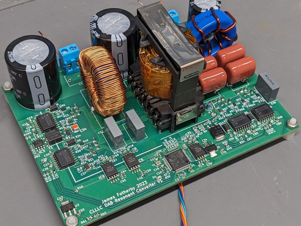
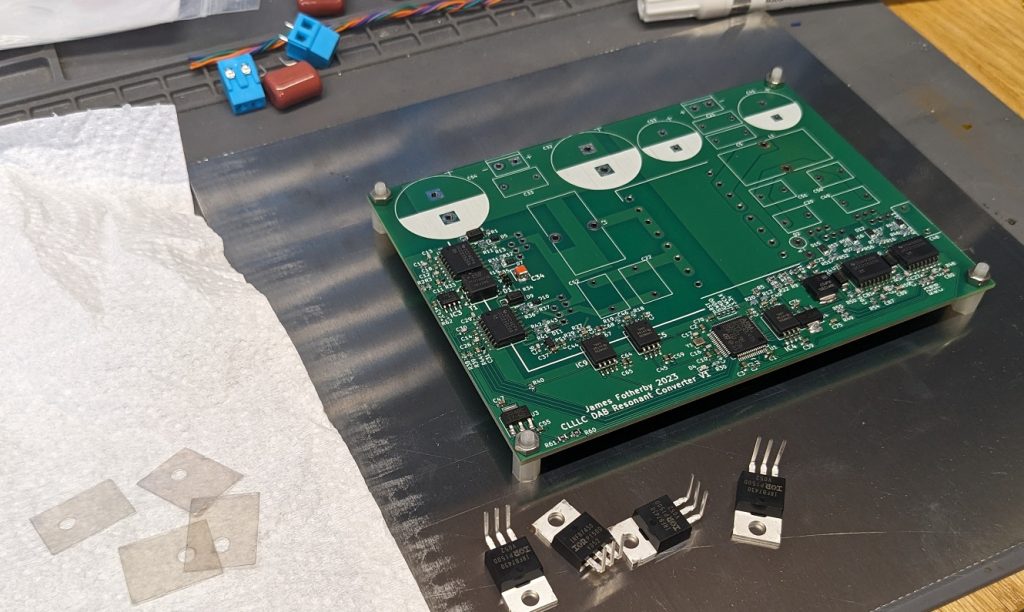
20nd July – Schematic finished, PCB routed and Assembled
Good progress recently. Everything is on GitHub. I finished the schematic and here’s the final version:
Here’s the BOM with links to suppliers
Discussion:
- I have followed the various chip application examples because I wanted everything to just work. I think many components could be done away with:
- I think the gate drive could be a simple resistor without the need for separate discharge diodes and resistors (ie get rid of D5 & R6 for each MOSFET – that’d get rid of 16 components)
- Perhaps I have been overzealous with the decoupling caps. Sprinkle them like candy has always been my motto but there do seem to be rather a lot.
- The low voltage resonant capacitor bank needed to be 8uF. This must handle an enormous amount of current (in the order of 25A RMS). I have never appreciated that capacitors have current limits before. I learnt about various film materials used and discovered Polypropylene (PP) capacitors have the lowest dissipation factor. Some dielectrics are more lossy than others and Wikipedia has a good section on Characteristics of film materials. The datasheet for the 2.2uF capacitors that build the resonant capacitor bank implies a permissible current of 7A each. This compares to about 2A for PET versions (substantially lower). As such I’m hoping the capacitors can handle the resonant current.
- Current sensing – Perhaps I have been daring only measuring current in 1 spot. With 25A RMS on the low side I did not want to insert any shunt resistors for fear of large losses. So I decided to place a shunt resistor on the ground return on the high voltage side as you can see in the schematic. I hope this’ll work ok.
- The low side voltage could be up to 30V. The digital logic, gate drive circuitry etc needs ~200mA. This is a lot of power to dissipate by the linear voltage regulators. I crudely added some resistors and a zener diode to help spread out the heat dissipation. Perhaps in future a small buck converter chip would be better.
- The components are as they are in the BOM
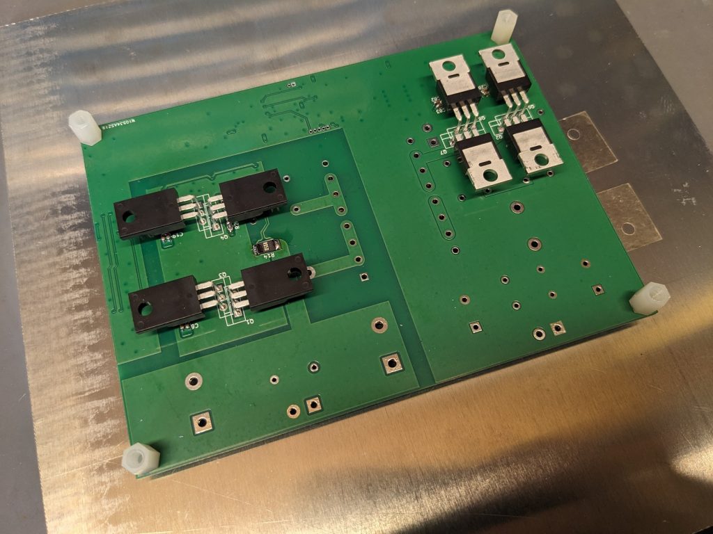
Here’s the PCB layout:
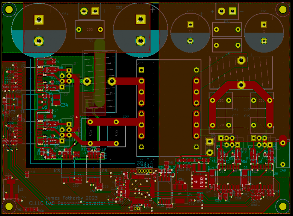
Discussion:
- I don’t understand how one is supposed to achieve appropriate clearances and track widths with these MOSFET packages!? Their legs are so close together. Presumably since they sell 600V TO-220 packages then the clearances are adequate?
- I fear that the current handling capacity of the traces on the low voltage side are inadequate. We’ll get 2oz PCBs and if they get hot I’ll beef them up with some copper wire.
- I ordered the PCBs from PCBWay. I like this company because they are very quick, well priced and produce quality and customizable PCBs. It’s a 2-Layer board.
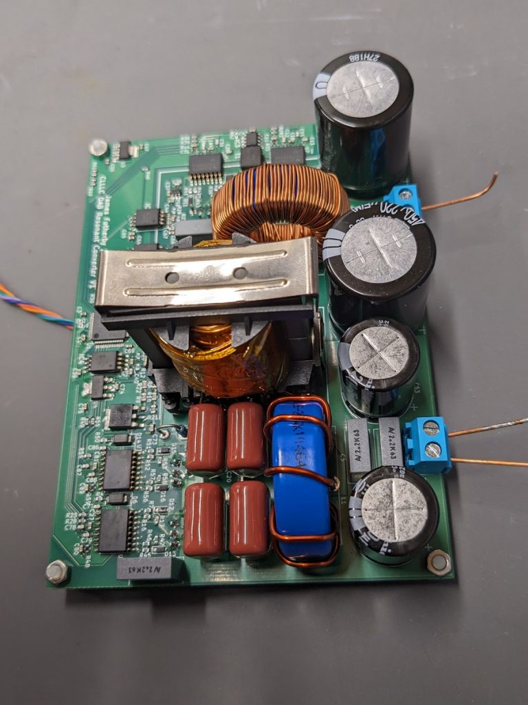
I wound another transformer:
- 5:77 Turns, Lp = 18.5uH, N = 15.3
- EDT39 Core with a 0.2mm gap
- I used a vertical bobbin for compactness on the PCB
- I have been getting all my cores from www.powermagnetics.co.uk
The inductors were hand wound. The MS-157125-2 is the larger high voltage core and the MS-130026-2 is the low voltage high current core.
Here are pictures following assembly of the PCB:

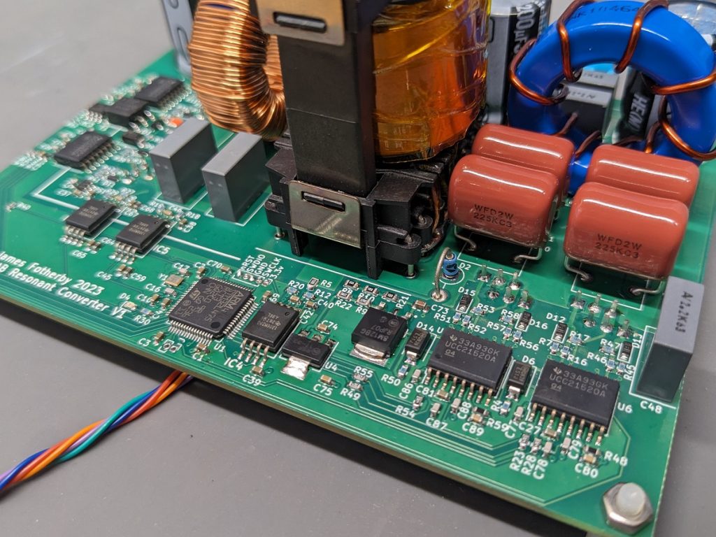
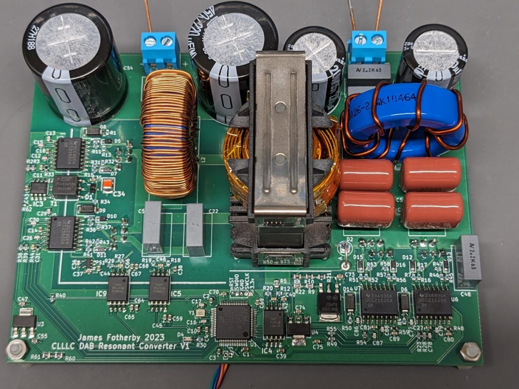
21st July – Initial Testing
I was delighted to find that everything worked as expected on powering up. Namely:
- The voltage regulators produced 12, 5 and 3.3V as expected
- The STM32L475 programs fine
- The MOSFETs switch as they should
- The sigma-delta modulators appear to be working nominally
- The circuit draws 190mA of current at rest.
13th December 2023
I have been up to other things and this project has been severely neglected. I did do several days of testing back in July. These circuits are complex and the difficulty is that there are so many variables. The “tweak and see” method begins to fall apart when you have so many different variables. I could get power transfer for a specific operating point but I couldn’t easily adjust the voltage gain. And when the load changes it effects the operating point too. Small changes in various inductances, capacitances frequencies can have non-linear effects.
To discuss:
- tried yet another transformer – need to choose a better core
- Software – compare mode, synchronising using timer 2
- unidirectionality, using HV MOSFETs just as diodes
- what next?
4 responses to “Bidirectional Resonant Converter”
-
Hello, how are you, I hope you are well,
I follow your developments, and I appreciate the way you provide a beginning, middle and end, with theoretical information along the way.
Please see the links below if you haven’t already seen them.I’m in Brazil, in the city of São Paulo, my training is in electronics, I have experience and study the development of switching sources and voltage inverters. I’m working on a 48VDC/220VAC/1000W scalable and synchronized power inverter. I have a good understanding of critical lay-out pcb techniques for switched energy.
Sorry for my English/google
https://pt.aliexpress.com/item/1005005861481009.html
-
It is very good opportunity to learn the LLC and bidirection inverter . If I can do something for your project, that would be great.
I can layout PCB , make the PCBA samples. All I do is free charge, including every components . If ok, contact me by email:
craig.jiang@wincomlcd.com -
Can you share the code used during initial testing?
-
lot of of effort for good work
Leave a Reply