
Over the last 2 years I have been trying to build a grid connected inverter. These devices fall squarely within the realm of power electronics which is a field that endlessly interests me.
I have had 5 attempts at trying to build such a system and have recently succeeded at my endeavours with a 600W transformerless inverter. The current waveform only has 3.8% THD.
My earlier attempts are linked below. I was ignorant back then so they are full of design errors and mistakes. I won’t cover the content discussed in Version 4. The gerber files and software is all on GitHub. I use KiCAD for the PCB design and STM32CubeIDE for the software development.
2nd March 2023 – How to improve on version 4
Two aspects that worked well in V4:
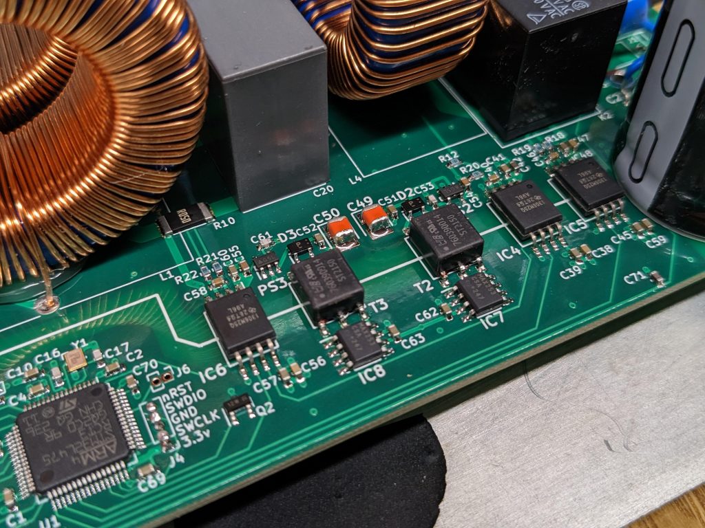
- The onboard STM32L475 – no flying wires.
- The AMC1306 isolated ADCs measured currents and voltages beautifully
There are a couple aspects I’d like to reconsider:
- Although the GaN MASTERGANs offer futuristic switching efficiencies, they are tricky to heatsink, they need a separate isolation barrier and they are harder to solder onto the PCB. I think I stand more chance of success using isolated gate drivers and TO-220 style MOSFETs.
- I think there should be more DC Bus capacitance onboard the PCB. I have never seen an inverter where the bulk capacitance is separate from the main PCB.
I plan to make only a few alterations to the PCB. I have just had a look into the variety of isolated gate drivers out there. Seems like all the big manufacturers (TI, Infineon, Analog Devices, ST) do their own versions. TI have some tools to help compare the various chips and I found some good articles:
- https://www.ti.com/power-management/gate-drivers/isolated-gate-drivers/overview.html
- https://www.powerelectronicsnews.com/how-to-select-the-right-gate-driver-for-your-sic-mosfet/
- IGBT & SiC Gate Driver Fundamentals – A superb whitepaper!
Following my research, I shall use the UCC21520ADWR which is currently in stock with DigiKey. I’m quite fond of the the MOSFETs I used in V3 – the 600V 0.094ohm STF35N60DM2.
I’ll get to work making the necessary changes to the PCB next.
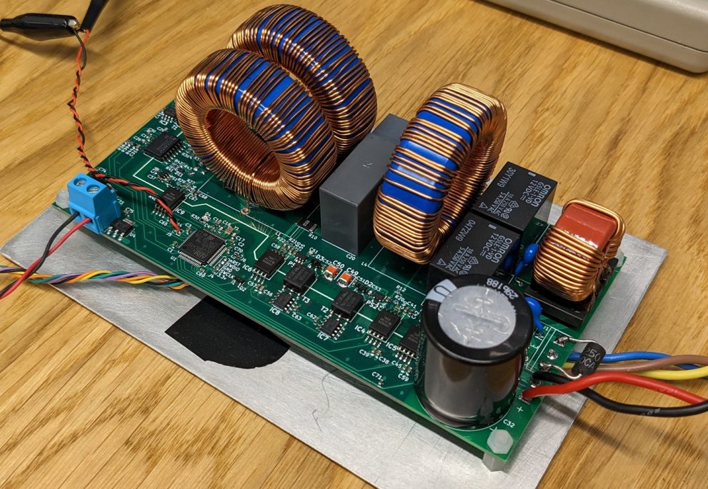
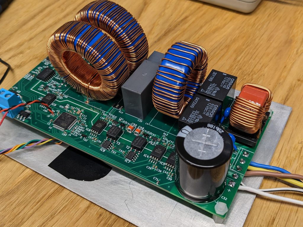
27th March – Schematic, PCB Routing and Assembly Finished
I tweaked the schematic to use through hole MOSFETs with UCC21520 isolated gate drivers.
Here as some of the other changes:
- The gate drive needs 12V so one of the mini-transformers is now a 5-12V rather than all 3 being 5-5V
- The through hole MOSFETs mount underneath and are bent to lie against an aluminium heatsink
- I have put a 220uF 450V electrolytic on the board – another 220uF can be on our DC Bus power supply
- I have changed the filter a little bit – more discussed later – I’m using Tina TI to simulate this.
- I had originally made a small error with the 2200pF EMI capacitors so I have corrected this
- The choke is bigger and better. It’s 2.2mH and can handle 6A.
- I removed unnecessary resistors from the analogue front ends of the AMC1306s.
I hope that’ll enable us to handle 1000W. The gerber files are on Github
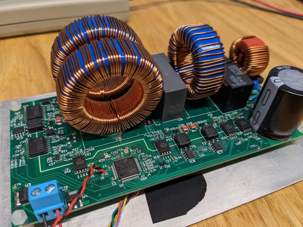
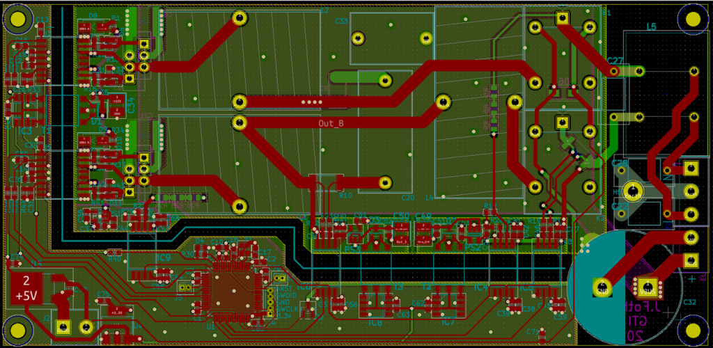
The dimensions of the 4-layer PCB have not changed from V4. PCBway manufactured the boards. I paid on the 16th, they were shipped in the 19th and they arrived on the 24th – incredible service!
The assembly went smoothly. It took 3-4 hours to do the stencilling and part placement.
I powered up the board and it all worked as expected. I have promised myself not to proceed until I have bombproof overcurrent and overvoltage cut-outs. I shall get the analogue watchdogs to disable the PWM signals by pulling the PWM_Disable line high in any erroneous situations!
29th March – Filter Design
The LCL filter must pass 50Hz (by having a low impedance at this frequency) and reject all the high frequency PWM switching frequencies.
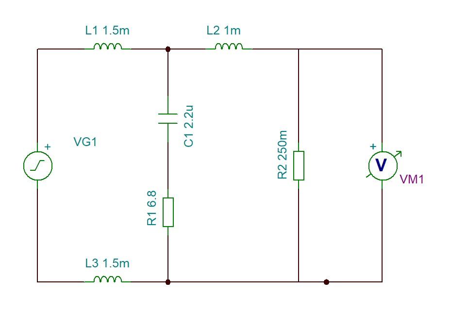
See the filter schematic used in this inverter iteration. (R2 represents the ~grid impedance). It involves:
- Inverter side inductance, Li (L1 & L3). Comprising 2 x 1.5mH inductors but you can think of it as single 3mH inductor
- The grid side inductance Lg (L2) = 1mH
- The filter capacitor, C = 2.2uF
- The filter resistor R = 6.8R
Step 1 – Choosing the values of Li, Lg, C.
Our component choices are based on these specifications:
- 240V, 50Hz grid
- PWM switching frequency of 40kHz
- Filter ripple current of 20%
- A bus voltage of 400V
- Rated inverter power output of 1000W
I followed this 5 minute video tutorial (https://www.youtube.com/watch?v=ZNUqGBBlKLI).
1) C is chosen such that it absorbs 50Hz reactive power at 5% of the rated power of the inverter. The video shows the necessary calculations but this results in needing a 2.7uF capacitor. I settled on a 2.2uF capacitor since it was easier to obtain. We want to use a 250VAC rated film capacitor (since they have low dissipation factors and stable capacitance values)
2) Li is chosen to limit the 40kHz ripple current through Li and C. This ripple peak to peak should typically be limited to 20% of the rated current. The ripple current changes depending on the instantaneous voltage the inverter is having to output but is maximal at 50% duty cycle (ie. when the inverter is outputting 200V from a 400V bus). A 1000W 240V output requires a peak output current of 6A. Therefore we should limit our ripple current to 1.2A.
You can use the calculations in the video. I also played around with this online ripple calculator. With a Vbus = 400V, output Vo = 200V and 40kHz switching frequency you can see you need 2.1mH.
Step 2 – Inductor design
Inductors tend to loose their inductance with a DC bias applied. We need to choose our inductor such that it still has 2.1mH even with a DC bias current of 6A.
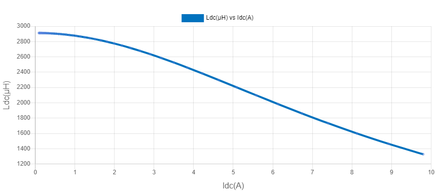

I chose to build the inductors using this core (FS-185090-2 from power magnetics). I used the Inductor Analyzer tool on the Micrometals website. This tool allows you to select the FS-185090-2 core and input the number of turns applied. I configured the tool for “AC inductor with ripple” and selected 2 series inductors in the “stack”. With 102 turns on each core and 2 in series we get a 2.9mH inductor. However with 6A applied the tool tells us that our overall inductance will have decreased to 2mH. Excellent – that’s about right.
3) Lg – The paper “Optimal design of LCL filter in grid-connected inverters” by Yong-Jung Kim, Hyosung Kim concludes “Through analysing frequency responses in LCL filters, the optimal inductance ratio is discovered that the inverter-side inductance should be three times as large as grid-side inductance” Based on this research I chose Lg = 1mH and I used the same inductor core.
Winding the inductors is a bit tedious (or therapeutic depending on what mood you’re in). I put 91 turns around the core and got an inductance of 1.08mH. This will be 800uH at 6A. I’m using 21AWG wire which is a little on the thin side. The resistance of this inductor was 200mOhm.
Overall our inverter has approximately 1Ohm of resistance amongst the 3 inductors, the PCB traces and the MOSFETs. At 4A RMS we can expect at least 16W of heat dissipation excluding switching losses.
Step 3 – Check Resonant frequencies and Simulate
It is important to ensure that the filter resonances are clear of any frequencies we shall be applying.
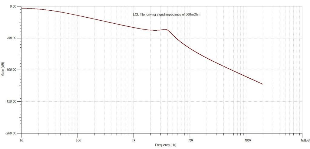
I simulated the LCL filter network on Tina. The grid presents an approximate impedance of 100-500mOhm at a socket outlet.
Tina plotted the filter attenuation for us and shows a damped resonance at 3.8kHz. I experimented with different filter resistors and 6.8ohms seems to give us a good compromise between blunting the resonance and attenuation of high frequencies. As the grid impedance changes, the resonant peak may vary slightly around this but hopefully not too drastically.
30th March – Just Realised I Need a TVS!
If the output is suddenly disconnected under load (or the fuse blows) the grid side inductor (Lg aka L4) will generate a voltage spike.
Lg could have 6A flowing through it. A 1mH inductor with 6A flowing contains 18mJ of energy. This has to go somewhere. At the moment the energy can only go into C22, C27, C28 (The three 2200pF EMI capacitors). 18mJ into a 3300pF capacitor will charge it to 3300 Volts! That’s going to cause some serious damage!
We need a transient voltage suppressor to clamp this voltage to below ~600V and dissipate this energy. I will get one.
It’s also important to consider what’d happed if the relays were to open under load. They never should since any fault condition will disable the MOSFETs significantly quicker than the relays could ever open. If they open under load then a voltage transient could occur between the output and DC Bus. This could cause some arcing between the relay contacts. I don’t think the issue is as significant as the former one because of the isolated nature of the AMC1306s.
Successfully Got Overcurrent/voltage Protection Working
I have been trying to use the DFSDM analogue watchdog to trigger an interrupt if an overcurrent/voltage situation arises. I had been failing to configure the peripheral DFSDM registers for months! I gave up in v4 (why it exploded) and used a 1ms periodic check on the output current instead (How ignorant I was thinking 1ms was an adequate sampling time!).
I have realised robust overcurrent and overvoltage protection is mandatory in inverters. I cracked the code a few days ago with inspiration from ChatGTP and the debugging features of STM32CubeIDE. (Answered on Stack Overflow linked above)
Anyway, we now have the DFSDM analogue watchdog monitoring the gird current (Ig) and the bus voltage (Vbus). The watchdog uses a sinc3 filter with an oversampling ratio of 16. To determine the sample rate this gives us we need to consider a few factors:
- Oversampling Ratio: The oversampling ratio is the ratio of the sampling rate at the input to the sampling rate at the output of the filter. In this case, the oversampling ratio is 16.
- Input Data Rate: The input data rate is the rate at which the bits are being sampled into the sigma-delta modulator. In this case, the input data rate is 10MHz.
- Filter Order: The order of the filter determines the number of taps required to implement the filter. In this case, the sinc3 filter has a filter order of 3.
- Resolution: The resolution of the output data is determined by the number of bits used to represent the output values.
Using the oversampling ratio and the filter order, we can calculate the output data rate as follows:
Output Data Rate = Input Data Rate / Oversampling Ratio * (Filter Order + 1)
Output Data Rate = 10MHz / 16 * (3 + 1)
Output Data Rate = 156.25kHz
Sinc3 filters have excellent transient response times. They can settle within 3 sampling periods of a step change. The application note by TI below is an excellent read on the topic.
A 156.25kHz sampling rate equates to a sampling period of 6.4us. This means within 20us we can respond to an overcurrent situation. This is about fast enough when you appreciate that 400V across a 4mH inductance causes a current rise of 100A/ms. In 20us the current could changed by 2A!
Now that over-IV protection is in place, experimenting with higher voltages and various control algorithms is far less stressful. Nothing bad should happen! (I can’t believe version 4 lasted as long as it did with an over-IV system having a 1ms response time!)
100W Grid Tie with a 25V Transformer
It’s always a nice milestone even if it is through a transformer. I supplied the inverter with a 50V bus voltage and have connected it to a 25-230V toroidal transformer. This confirmed the operation of the PLL and current control algorithms.
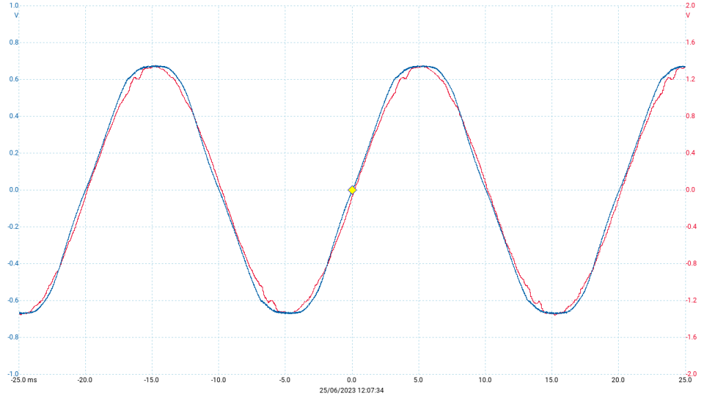
In these images we can see the 100Hz and 40kHz ripple in the bus voltage. The blue trace is our AC coupled bus voltage (50V/V) and the red is the injected grid current (4A/V). In these snapshots you can see we’re outputting 3.4A RMS into the 25V transformer.
So we’re getting 1V peak-peak 100Hz ripple (This was with 2200uF bus capacitance). You can see the high frequency 40kHz switching ripple too which is 500mV peak to peak. Thoughts:
- Would be interesting to see the amplitude of the 100Hz ripple for different bus capacitances
- This is a lot of ripple! Is this normal?
- We need to take our bus voltage up to 400V.
13th April – 240V Sine Wave Inverter
I have thoroughly tested the overcurrent and overvoltage cut-outs. These are working flawlessly and have been reliably disabling the H-Bridge drivers above the cut-out thresholds I have set.
Now that over-IV protection is in place, experimenting with higher voltages and various control algorithms is far less stressful. Nothing bad should happen!
Yesterday I increased the bus voltage to 400V and output a 230V sinewave into a 200ohm load. The inverter handled 260W comfortably. I got the PR controller regulating the current so that it was independent of bus voltage.
I next connected the grid to the inverter. The PLL works flawlessly (It always has). I tried many different parameters for the PR controller but I just couldn’t get the inverter to engage with the grid. The H-Bridge would engage at a zero crossing point and the PWM would commence but then a ~1.1kHz oscillation grew until after a few milliseconds the over-IV would trip out. I’m sure this is something I can address but I had no luck after several hours. I tried adjusting various control parameters and gains to no avail.
Let’s summarise where we are:
- We have a voltage source inverter that can take a 400V bus and comfortably generate a 240V waveform
- All of our voltage and current measurements appear accurate with good SNR
- We have over-IV protection that operates within 20us to protect against any damaging conditions
- Our PLL works flawlessly so we know the exact phase and frequency of the grid 50Hz fundamental
- We are connected directly to the grid however our current controller is not working yet. An oscillation occurs after engagement and grows until the system trips out.
23rd June – 600W Grid Connected Inverter!!!
Absolutely smashed it! We have managed to inject over 600W into the grid with no transformer and a sinusoidal current waveform containing only 3.8% THD.
A few key changes were made to bring everything together:
1) Enable auto-reload preload
Previously, I used timer 4’s overflow to call the PLL interrupt function at 3.2kHz. This would iterate the PLL and increment our phase counter. The counter period (nominally 1000 for 50Hz) is slightly adjusted by the PLL’s PI controller. Here’s the old code:
void PLL()  {
   int32_t Signal_Multiple = (int32_t)(Cos_LookupF[_50_Index] * V_grid);
   PLL_PID.input = Integral(Signal_Multiple);
   PIDCompute(&PLL_PID);

   TIM4->ARR = SINE_STEP_PERIOD + (int32_t)PLL_PID.output;
   _50_Index++;

   if(_50_Index == SINE_STEPS)
      _50_Index = 0;
}
It’s important to enable the auto-reload preload function of the timer since we are adjusting the auto-reload register on the fly. This buffers any new ARR writes until the timer counter is 0. This avoids ever accidentally writing an ARR value less than the immediate counter value. Since the counter is always counting upwards, if this were to happen then no compare match would occur until the counter rolled over. This could cause a significant delay and upset the program flow.
The timer 4 ISR (and hence PLL function) is triggered on overflow so this situation should never happen but we should enable the pre-load just in case.
2) Use Timer 5 as our phase counter
Rather than using a global variable (_50_Index) as our phase counter I have configured timer 5 to do the same job. Timer 5 is clocked automatically by timer 4’s overflow. Timer 5 is now our phase counter and counts from 0 to 63 before automatically rolling over. This modification reduces the jitter in the phase counter and keeps things cleaner. Our resulting PLL() code is now:
void PLL()  {
   float V_grid = ((float)V_grid_DMA) * V_GRID_SENSOR_K;
   int32_t Signal_Multiple = (int32_t)(Cos_LookupF[TIM5->CNT] * V_grid);
   PLL_PID.input = Integral(Signal_Multiple);
   PIDCompute(&PLL_PID);
   TIM4->ARR = SINE_STEP_PERIOD + (int32_t)PLL_PID.output;
}
Whenever a local oscillator value is required we simply use Timer 5’s count (ie. our phase count) as a lookup index in our sine table:
const float Sin_LookupF[65] =
{
   0.000000,0.098017,0.195090,0.290285,0.382683,0.471397,0.555570,0.634393,
   0.707107,0.773010,0.831470,0.881921,0.923880,0.956940,0.980785,0.995185,
   1.000000,0.995185,0.980785,0.956940,0.923880,0.881921,0.831470,0.773010,
   0.707107,0.634393,0.555570,0.471397,0.382683,0.290285,0.195090,0.098017,
   0.000000,-0.098017,-0.195090,-0.290285,-0.382683,-0.471397,-0.555570,-0.634393,
   -0.707107,-0.773010,-0.831470,-0.881921,-0.923880,-0.956940,-0.980785,-0.995185,
   -1.000000,-0.995185,-0.980785,-0.956940,-0.923880,-0.881921,-0.831470,-0.773010,
   -0.707107,-0.634393,-0.555570,-0.471397,-0.382683,-0.290285,-0.195090,-0.098017,
   0.000000
};
However that alone would only provide a low resolution stepped LO value. To improve significantly upon this we can use interpolation to get a good LO_Sample for our current controller setpoint:
// Interpolate our LO steps to get a more accurate LO sample:
uint32_t Timer4_CNT = TIM4->CNT;
uint8_t Lookup_Index = TIM5->CNT;

float diff = Sin_LookupF[Lookup_Index + 1] - Sin_LookupF[Lookup_Index];
float Timer4_CNT_Ratio = 0.001f * (float)Timer4_CNT;
float LO_Sample = Sin_LookupF[Lookup_Index] + (diff * Timer4_CNT_Ratio);
3) Faulty Resonant controller code
I began to suspect that the code implementing the PR controller wasn’t behaving as expected. I discovered a website (Ramblings from Hao) and his associated PR implementation which looked better. I decided to replace the code I was using with his. Here’s a graph from his website showing how his resonant controller responds to an error signal. Do check the links for more information.
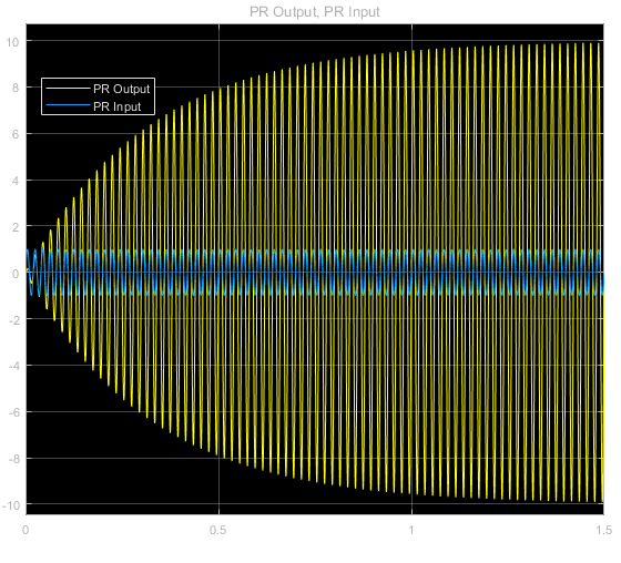
This is the behaviour I expect. And for error signals away from the resonant frequency the amplitude of the output is less.
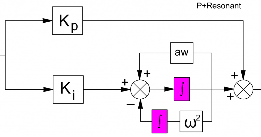
This is the block diagram of how the PR controller is implemented. This is taken from p33 Active damping of LCL Filter Resonance in grid connected inverters which is a good read on the topic of PR controllers too.
4) Feedforward control
Resonant controllers take time to build resonance. When the inverter joins the grid at a zero-crossing-point it must start replicating the grid voltage immediately. I solved this problem with the addition of a feedforward term. The code below shows our entire current controller:
// -------------- 1) Iterate our PI Controller:
I_OUT_PID.setpoint = LO_Sample * P_OUT_PID.output;
I_OUT_PID.input = I_grid;
PIDCompute(&I_OUT_PID);

// -------------- 2) Iterate our Resonant Controllers:
float Ui_50 = pr_calc(&PR_50, I_OUT_PID.setpoint, I_grid, 2 * 3.1415926 * 50.0);
float Ui_150 = pr_calc(&PR_150, I_OUT_PID.setpoint, I_grid, 2 * 3.1415926 * 150.0);
float Ui_250 = pr_calc(&PR_250, I_OUT_PID.setpoint, I_grid, 2 * 3.1415926 * 250.0);
float Ui_350 = pr_calc(&PR_350, I_OUT_PID.setpoint, I_grid, 2 * 3.1415926 * 350.0);
float Ui_450 = pr_calc(&PR_450, I_OUT_PID.setpoint, I_grid, 2 * 3.1415926 * 450.0);
float Ui_550 = pr_calc(&PR_550, I_OUT_PID.setpoint, I_grid, 2 * 3.1415926 * 550.0);

// -------------- 3) Iterate our Feed-forward Controller:
float Feedforward = LO_Sample * 358.0;

// -------------- Add together the various control outputs:
float Demanded_Output_Voltage = Feedforward + I_OUT_PID.output + Ui_50 + Ui_150 + Ui_250 + Ui_350 + Ui_450 + Ui_550;
The output current is controlled by 1) A PI controller (The integral gain is very small and mainly used to prevent any DC currents from flowing) 2) Our resonant controllers which also compensate for all the harmonics in the grid voltage and 3) a 253V sinusoidal voltage term.
The feedforward term contributes >95% of the output signal. It approximates the grid voltage and the other controllers work to reduce the amplitude to prevent too much current being injected. I discovered it was better to overapproximate the grid voltage rather than underapproximate it. The inverter is fully bidirectional but our DC bus generator is not. If the inverters output voltage is less than the grid voltage then current flows into the inverter. This raises the bus voltage and on a number of occasions caused the over-V protection system to activate (set to 445V)
With this feedforward filter in place there is no need for the resonant controllers to build resonance when joining the grid. The output voltage is already approximately correct and the resonant controllers only have to slightly adjust the signal amplitudes to drive the correct current.
4) Interrupt priorities
Because the STM32L475 has a nested interrupt controller we don’t need to worry about having long interrupt service routines. We need our controller function running like clockwork so it’s set to pre-empt other interrupt service routines. (Naturally the DFSDM analogue watchdogs responsible for our over-IV protection system have the highest pre-emption priority).
void HAL_TIM_PeriodElapsedCallback(TIM_HandleTypeDef *htim) {
   if (htim == &htim3)
      Controller();

   if (htim == &htim4)
      PLL();

   if (htim == &htim2)
      Grid_Checks();
}
The main loop has no code in it. All processing is done within ISRs which is tidy. I thought it important to measure how long each function takes to run to avoid pushing the processor beyond what it can manage which would be catastrophic for timings:
- Controller(): 16us
- PLL(): 7us
- Grid Checks(): 12us
The processor is idling >50% of the time so we have plenty of processing power remaining.
5) Bus voltage upgrades
I upgraded the previous 20kHz switcher I was using to this beefier one. The new one can take up to 32V at the input. With 30V applied the setup below behaves as a 412V voltage source in series with approximately 25 ohms. If you start pulling current the voltage drops due to the internal resistance.
It shouldn’t go without mention that this high voltage power supply is dangerous. There’s exposed metal at over 400V. It’s not bidirectional and it’s not especially efficient but it was quick, easy and does the job. I am daydreaming about building a bidirectional CLLLC resonant converter to round this whole project off.
6) PI Output current control
A PI Controller is employed to regulate the current injected into the grid. More current is injected until the bus voltage drops down to 370V. This allows me to vary the injected power by adjusting the voltage fed to the bus generator from my 30V 30A lab power supply.
// Here we adjust our output current to keep our bus voltage at 370V using a PI controller
P_OUT_PID.setpoint = 370.0f;
P_OUT_PID.input = V_bus;
PIDCompute(&P_OUT_PID);
A few further tests:
The waveform below shows the grid voltage (500V/V) and the output current (3A/V). This demonstrates a 690W injected power. My spectrum analyser measured 3.8% THD.
I should measure efficiency more precisely but the inverter board and aluminium heatsink itself is only reaching 30 degrees above ambient. I suppose the MOSFET deadtimes are incredibly short and the gate drive is strong.
The downside to this powerful hard-switching is enormous amounts of EMI. I have done my best to supress the EMI in my PCB design but regardless a lot leaks out (probably the inductors). EMI is so large that the digital communications between the debugging/programming board is corrupted. This stops you from debugging the board on the fly – normally you can watch variables on a computer whilst the processor is running and set breakpoints etc. Code uploads fine because this is done under reset. I have resorted to getting most of my debug information from a scoped DAC output.
What’s Next
I don’t know. I have achieved my goals with this project. I don’t have a specific application I need it for yet. One day I’d like to set up my own grid connected battery bank but I’ll need an inverter of at least 2000W to be useful. It was predominantly a research project for me to explore the area. I have learnt enormous amounts and built up many intuitions such as:
- PCB design strategies for reducing EMI and gate drive resonance.
- Inductor core design factoring in saturation, core losses, choosing a core permeability etc
- Implementation of resonant controllers to control sinusoidal current signals
- DFSDM
- LCL filter design and the need for damping to avoid resonant peaks.
- And much more
I have only just scratched the surface of this field. When I compare my work to that of established engineers developing EV chargers, motor drivers, computer PSUs etc, my work is laughably simple. How I wish I could work within such a team of engineers (If anyone knows of any job offers for me…)
Thoughts for future:
- I could try GaN FETs again and use 100kHz PWM with much smaller inductors to see how small and efficient I could build a 750W inverter
- I’m not using the relays or the capacitor current sensing at all so I could remove quite a few components and maybe half the board size?
- Or I could work to increase power output to something more useful like 2.2kW
- I’ve read about active damping, I could look into this but the LCL damping resistor doesn’t seem to cause many losses…
- The inverter needs supplying with a bus voltage of 370-420V. I’m interested in bidirectional DC/DC resonant converters.
- I’m interested in swapping the PR current control for something more sophisticated. I’m interested in model predictive control systems and enjoyed reading this PhD thesis on the subject (Model Predictive Control of a Grid-Connected Converter With LCL-Filter by Joanie Michellene Claudette Geldenhuys)
23 responses to “600W Grid Connected Inverter – V5”
-
Looking for some working models at a cost, shipping to India. Please let me know
-
Hi James,
Nice project you have here. Thank you for documenting it so thorougly as it is also a subject that interests me greatly.
I started reverse engineering an old solar invert to try to experimenting with grid tie inverters.One good idea I think would be to add two relays to the output as a further safety precaution when you start operating in grid tie mode.
They might be slow to switch, but can operate if the mosfets break down or something. And you can first synchronise to the grid with the relay open and then close it when the waveform is build and synced.Instead of a TVS, a MOV is usually used for overvoltage protectionin AC situations.
Good luck with your project, I will keep following it. Any way to add it to an RSS feed?
-
Thanks for your comment btw. It took me a long time to get to grips with all the concepts behind this project. But I feel I have conquered it at last. This implementation does have two relays on the output. I intended to use these as a safety precaution but actually they are not being utilised by the software at present. The TVS here is needed to prevent fast inductive spikes if the output fuse were to blow. I think a TVS works better than a MOV. Do you not agree?
-
-
This is really interesting, I’m trying to do something similar but only just scratching the surface with Control.
What’s your background? -
I cannot thank you enough for putting this information out there. I’ve actually been on and off researching making an inverter like this for off-grid use since at least 2018, but I never got nearly this far. I couldn’t even figure out the LC filter! Every combination of L and C values always got me a resonance. Since then I’ve certainly learned a bit and it looks like a bunch of people have succeeded at making DIY sine inverters, but yours is the first homemade grid tie I’ve seen!
My goal is to be able to run multiple inverters in parallel at multiple generation locations (i.e., wind, solar, hydro). Basically like a mini grid. I’m curious, what do you think it would take to make this into a hybrid inverter (capable of both on and off grid use?)
Also, are you using that choke as an isolation transformer, or am I just misreading the schematic? Cause if so that’s genius.-
Hi, thanks for your comment and sorry it’s taken so long to reply. There’s a lot to these inverters and it took me a long time to work it all out and 5 attempts. I should make a version 6 at some point – I want to make a fully bidirectional system that can charge/discharge batteries from/to the grid. For that I just need a bidirectional DC/DC stage to convert between the battery voltage and grid voltage. I hope to do this in the next year.
To answer your questions. Running multiple inverters in parallel should work in theory. If it was all off grid then you’d need 1 master non-grid tie inverter to set the 50Hz frequency and voltage. All other inverters would then grid tie to this and only inject power if the voltage fell. The slave inverters may work better as voltage source inverters rather than current source. Such a network could get complicated.
Using this inverter as an off grid inverter is easy – easy software change. The choke isn’t for isolation. Isolation is done by the DC/DC front end.
-
-
Great project!
Is it running stable and well now?I am looking for a grid-tie inverter for a windmill.
So please, if there is a chance to buy one, please let me know!Wolfram.
-
arguably this is all still a work in progress. I need to build the DC/DC converter to power this board
-
-
Just found your work looking for dyi grid tie inverters and want to thank you profusely for sharing this information. Would love to invest in your work should you ever want to take it to market. Not sure if you have checked pricing on these kinds of things but just priced out a 300Kw grid tie unit at over 76k usd. I think what you are doing is a great service sharing the process and the math/science/engineering as there is definitely a need to get this out there and it would be very encouraging to those considering getting started in green energy to know how it works and not be intimidated. I know from walking through your versions I have learned much already that had been unknown to me. Thank you again 🙂
-
Hi welcome dear friend
Ineed your contact
Please +923483428823
Please -
Dear James, thank you for your precious sharing.
Is there a way to limit the output power in relation to an input signal like 0-10V or 4-20mA?
In other words, is there the possibility to upgrade your GTI to GTIL (Grid Tie Inverter with Limiter)?Thank you so much
-
This is such an incredibly cool project! I see that you are working on an Isolated DCDC frontend as well, yet I’d assume long term it would be greater to have a single stage isolated topology for lower part count, cost and complexity. So happy you switched from Eagle to KiCAD (I did the same)
Have you considered tackling a more unified approach for the next inverter? I already like your component choice and would love to support you on the hardware side. Infineon an TI have some resources on microinverters as well
https://www.infineon.com/cms/en/applications/renewables/photovoltaic/micro-inverter-solutions/ -
Dear James
I’ve been closely following all your Grid Tie inverter versions, and I truly appreciate your continuous efforts and improvements.
I’m planning to build Version 5.0 and wanted to check if the STM32 source code is finalized. I noticed some code fragments related to Version 5 on your website (https://jamesfotherby.com/).
Additionally, if I want to control the reactive power injected into the grid, is there an easy way to achieve this using the existing source code?
Looking forward to your insights.
Best regards,
Adam Adam -
Nice job brother. Please if one want to convert this grid tie inverter into off grid inverter, what and where to make changes in the code?. I think if one can make this change, the inverter can do off grid system.
-
Off grid inverters are much more straightforward. Only a few lines of code need to be commented out.
-
-
To mitigate EMI generated by hard switching, it is recommended to implement a snubber across the MOSFET’s drain-source terminals, or adopt soft-switching (ZVS) methods to reduce both EMI and switching losses.
-
I’m following your lead now.
I’m having trouble with the system stopping after 2 seconds of power supply.
What should I do? Please reply.
-
Please contact me back tsw.tele@gmail.com
I ordered a PCB from your Github.
I assembled the circuit as you suggested.
I ran into a minor issue:
When I turned it on,
the circuit only worked for about two seconds and then shut down.
-
Dear James,
I am highly interested in grid-tied inverters and am currently focusing on inverters utilizing model predictive control (MPC). I would be delighted to engage in detailed discussions with you. Would it be possible to obtain your email address to facilitate more in-depth communication?
Thank you for your time and consideration.
-
Kudos on a great project. Can you share how fast the inverter can determine grid loss and shutoff?
-
In the GTI V2 instructable I included some images of the anti-islanding detection. It was about 120 ms there but it is configurable in software.
-
Thanks the pointer. That looks good. Looking forward to see you add the DC/DC converter.
-
-
-
It was not successful. I followed your instructions, ordering the PCB and all the necessary parts for assembly. I encountered a problem: when connecting to the grid, the system shuts down and resets after 2 seconds. I don’t know what to do. Please contact me for assistance at tsw.tele@gmail.com
Leave a Reply